A3986
Dual Full-Bridge MOSFET Driver with Microstepping Translator
Features
- 2-wire step and direction interface
- Dual full-bridge gate drive for N-channel MOSFETs
- Operation over 12 to 50 V supply voltage range
- Synchronous rectification
- Cross-conduction protection
- Adjustable mixed decay
- Integrated sinusoidal DAC current reference
- Fixed off-time PWM current control
Description
The A3986 is a dual full-bridge gate driver with integrated microstepping translator suitable for driving a wide range of higher power industrial bipolar 2-phase stepper motors (typically 30 to 500 W). Motor power is provided by external N-channel power MOSFETs at supply voltages from 12 to 50 V.
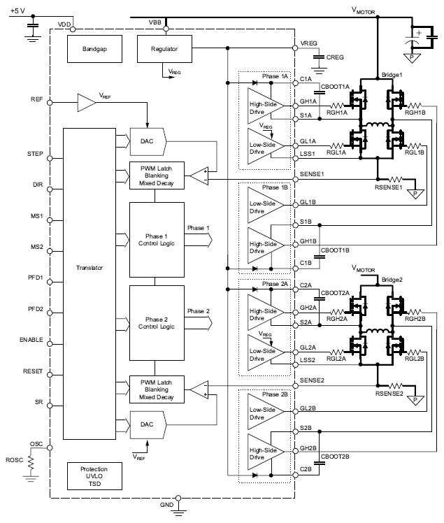
This device contains two sinusoidal DACs that generate the reference voltage for two separate fixed-off-time PWM current controllers. These provide current regulation for external power MOSFET full-bridges.
Motor stepping is controlled by the two-wire step and direction interface, providing complete microstepping control at full-, half-, quarter-, and sixteenth-step resolutions. The fixed-off time regulator has the ability to operate in slow-, mixed-, or fast-decay modes, which results in reduced audible motor noise, increased step accuracy, and reduced power dissipation.
The translator is the key to the easy implementation of this IC. Simply inputting one pulse on the STEP input drives the motor one step (full, half, quarter, or sixteenth depending on the microstep select input). There are no phase-sequence tables, high frequency control lines, or complex interfaces to program. This reduces the need for a complex microcontroller.
The above-supply voltage required for the high-side N-channel MOSFETs is provided by a bootstrap capacitor. Efficiency is enhanced by using synchronous rectification and the power FETs are protected from shoot-through by integrated crossover control and programmable dead time.
In addition to crossover current control, internal circuit protection provides thermal shutdown with hysteresis and undervoltage lockout. Special power-up sequencing is not required.
This component is supplied in an 38-pin TSSOP (package LD). The package is lead (Pb) free, with 100% matte tin leadframe plating.
Functional Block Diagram
